
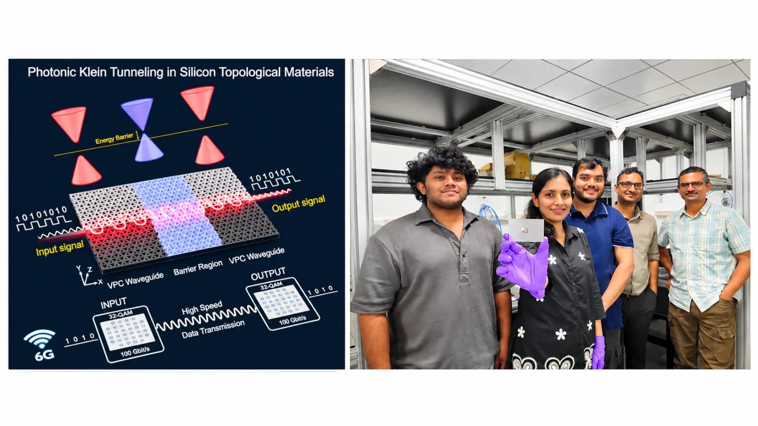
Researchers at the Jawaharlal Nehru Centre for Advanced Scientific Research (JNCASR) have developed a silicon chip capable of transmitting terahertz waves through engineered barriers with minimal signal loss, achieving data speeds of up to 100 gigabits per second (Gbit/s), a development that could support future 6G communication networks.
The research, conducted at JNCASR, an autonomous institute under the Department of Science and Technology (DST), demonstrates a potential approach to developing compact, high-speed terahertz circuits.
Future sixth-generation (6G) wireless networks are expected to operate at terahertz frequencies, which lie between microwaves and infrared light and offer substantial bandwidth. However, guiding these waves through compact circuits remains challenging, as bends, junctions and structural changes can cause signal scattering and reflection, reducing transmission efficiency.
To address this challenge, researchers used topological photonics, designing a silicon photonic crystal with triangular holes arranged in a pattern resembling graphene’s honeycomb lattice. The structure allows terahertz waves to travel along boundaries between different regions while resisting certain types of backscattering.
The team introduced an engineered barrier by modifying the sizes of triangular holes along a short section of the waveguide. Tests showed that a single barrier caused only about 1–2 per cent signal loss, while two consecutive barriers resulted in losses of around 2–3 per cent.
In comparison, similar barriers in conventional, non-topological waveguides significantly reduced signal transmission.
Researchers found that transmission remained close to barrier-free levels when the barrier strength was below a characteristic coupling strength of the photonic crystal, providing a potential design principle for future devices.
The team fabricated three devices using high-resistivity silicon, a material compatible with established semiconductor manufacturing processes. These included a waveguide with two consecutive barriers, an omega-shaped structure featuring four sharp bends and a central barrier, and a power splitter with a barrier in one of its branches.
Measurements conducted across frequencies of 310–360 GHz closely matched simulations. In the power splitter, both output signals remained nearly identical, indicating that the barrier had minimal impact on transmission.
During high-speed data transmission tests, the double-barrier and omega-shaped devices achieved speeds of 48 Gbit/s and 60 Gbit/s, respectively. The power splitter supported transmission at 100 Gbit/s using QAM-32 modulation, which encodes information through variations in signal amplitude and phase.
At this speed, a 5-gigabyte high-definition film could theoretically be transferred in less than half a second.
The study was led by Dr Abhishek Kumar, Assistant Professor at JNCASR and head of its Meta Optics Laboratory (MetoLab), with Samina Mulla and Sangram Kumar Sadhu serving as joint first authors.
Other collaborators included Asif Iqbal M and N. S. Vidhyadhiraja from JNCASR; Siddhartha Lal from IISER Kolkata; Anshuman Kumar from IIT Bombay; Zhonghua Gu and Prakash Pitchappa from the Institute of Microelectronics, A*STAR, Singapore; and Pascal Szriftgiser and Guillaume Ducournau from the University of Lille and CNRS, France.
“Showing that terahertz waves can cross a barrier created simply by changing the hole geometry, while carrying 100 gigabits per second, suggests that this effect can become a useful design tool for terahertz chips,” said Dr Abhishek Kumar.
The findings could pave the way for compact terahertz circuits capable of routing and splitting high-speed signals on a single chip with minimal transmission loss.
Researchers now plan to explore ways to control the barriers electrically, thermally or mechanically, potentially enabling devices to redirect signals between different pathways on demand.
The study has been published in the scientific journal Advanced Materials.
Published: Thursday, 5 November 2026 | 3:25 PM IST